| IBM's current high-end microprocessor, the P2SC Super
Chip, is a hard act to follow. After all, it's the
microprocessor that IBM used in a supercomputer to beat
world chess champion Garry Kasparov last year. But the new
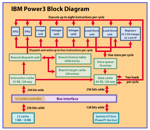
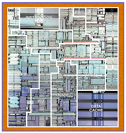
Power3 processor is even more awesome. Imagine a 64-bit CPU with 15 million transistors, eight functional units, a 128-bit wide system I/O bus, a 256-bit wide secondary cache bus, nearly 8 GBps of aggregate bus bandwidth, 128-way caches, and built-in support for symmetric multiprocessing (SMP). You won't have to imagine it for long. IBM produced the first silicon samples in early 1997. The Power3 will first be made with a hybrid 0.25/0.35-micron process called CMOS 6S2, which uses aluminum for the five layers of metal interconnects. IBM plans to have Power3-based systems in production in the second half of 1998. 64-Bit Architecture The Power3 is designed for high-end RS/6000 workstations, servers, and supercomputers. It adopts the 64-bit architecture and SMP features of the PowerPC 620. The Power3 stands to benefit more from a 64-bit architecture because it is aimed at an entirely different market than other PowerPC chips. "It's a server and workstation part, not a desktop PC part," says Mark Papermaster, Power3 product manager. "It'll really cook on huge engineering, scientific, and on-line transaction processing applications." The most dramatic measure of how IBM optimized the Power3 for large applications is the chip's phenomenal bus bandwidth. The system I/O bus is 128 bits wide — twice as wide as the bus on most of today's CPUs. At a clock frequency of 100 MHz, the Power3's system bus delivers 1.6 GBps of peak bandwidth. Not stopping there, the Power3 also has a private bus for the Level 2 (L2) cache, similar to the L2 backside bus on a PowerPC 750, Pentium Pro, or Pentium II. But while Intel's backside bus is 64 bits wide, the Power3's bus is an incredible 256 bits wide. At 200 MHz, that's 6.4 GBps of peak bandwidth — or a grand total of 8 GBps of aggregate bandwidth when added to the capacity of the system I/O bus. Furthermore, all that bandwidth is available for data. Each bus uses separate address, data, and control lines instead of multiplexing the control signals and addresses with the data, as most other processors do. Those extra lines, not to mention the superwide buses, boost the pin count far beyond the limit of what would be practical on a chip designed for mainstream PCs. The Power3 has 1088 pins, with 748 of them dedicated to signal I/O. Instead of cramming that many pads around the periphery of a die that's 270 square millimeters, IBM manufactures the Power3 with its patented C4 "solder-bump" technology, which distributes the pads all over the surface of the chip. The Power3's system I/O bus can run at clock ratios of 1:2, 1:3, or 1:4 with the core. The private L2 bus can run at ratios of 1:1,1:2, or 1:3. IBM says initial versions of the Power3 will run at a core frequency of more than 200 MHz. At that speed, it would make sense to clock the system I/O bus at 100 MHz and the L2 cache at 200 MHz. On more advanced fabrication processes, the Power3 core could run as fast as 400 MHz while maintaining the system I/O bus at 100 MHz and driving the L2 cache at 200 or even 400 MHz — if the static RAM (SRAM) chips in the cache could keep up. Until now, IBM's Power chips have always been known as "brainiacs": They achieve high performance through complex parallelism, not raw clock speed. The P2SC, for example, runs at a relatively pokey 135 MHz. But when the Power3 moves to IBM's CMOS 7S process (it replaces the aluminum traces with copper), 500 MHz will be a realistic possibility. This places the Power3 squarely in the "speed demon" category. Such a part will probably need higher clock divisors to drive the buses at manageable speeds. Peeling Open the Core The Power3, like Deep Blue's P2SC, is a wide superscalar machine highly optimized for floating-point math. It has two floating-point units (FPUs), three integer units, two load/store units, and a branch/dispatch unit. Given an ideal instruction stream, the Power3 can execute up to eight instructions per clock cycle, but it can retire only four per cycle. If some of those instructions are fused multiply-adds (FMAs), the Power3 can execute the equivalent of 10 instructions per cycle. That's because each pipelined FPU can execute the multiply and add operations of an FMA instruction in parallel, yielding a maximum throughput of four FP operations per cycle. FMA is IBM's term for single instructions that combine multiply and add instructions. FMAs are similar to the multiply-accumulate (MAC) or multiply-add (MADD) instructions found in digital signal processors (DSPs) and other CPUs optimized for data-intensive tasks. Each FPU also has special subunits for executing divide and square-root operations in hardware. All FP data paths are 64 bits wide (IEEE-754 double precision). Most floating-point instructions have a three-cycle latency and a single-cycle pipelined throughput. The architectural set of 32 FP registers is supplemented with 24 additional physical registers plus eight virtual registers. So, from the CPU's point of view, there are 64 FP registers to play with — transparently mapped to the architectural set of 32 registers. Two of the integer units execute single-cycle instructions (the majority), while the third integer unit handles more complex instructions. The nominal length of the integer pipeline is five stages. Here, too, register remapping expands the architectural set of 32 integer registers into a file of 64 registers. However, only 16 of the extra registers are actual physical registers — unlike the FP set, which has 24 additional physical registers. To keep all those functional units busy, the Power3 has extraordinary Level 1 (L1) caches and load/store capabilities. The load/store units can perform two loads or one store per cycle, and they can load data speculatively. Four ports on the data cache can simultaneously handle two 8-byte loads, one 8-byte store, and a 128-byte cache-line update in a special reload buffer. Although the caches are respectably large — 32 KB for instructions and 64 KB for data — addressability is their standout feature. Each cache is 128-way set-associative and holds 128 bytes per line. Therefore, the instruction cache consists of only two sets, and the data cache has only four sets (128 lines per set x 128 bytes per line = 16 KB per set). Each set is fully associative, so cache access is very efficient indeed. In contrast, the P2SC's data cache was twice as large (128 KB) but only four-way set-associative. What all this adds up to is superlative performance. IBM estimates that the Power3 will score 11-12 SPECint95 and 28 SPECfp95 at 200 MHz. Although the integer performance is about the same as a 300-MHz Pentium II (which scores 11.6 on this benchmark), the Power3's estimated FP performance is almost four times greater than the Pentium II's (7.2 SPECfp95). Of course, the Pentium II is shipping today and the Power3 isn't. But since IBM has actual silicon samples running in the lab above 200 MHz, you can bet those estimates are pretty accurate. When this chip moves to the CMOS 7S process, it'll really come into its own. Assuming that its performance scales with the clock speed, a Power3 running at 500 MHz could achieve a stunning score of 30 SPECint95 and 70 SPECfp95. IBM Power3 Block Diagram 15 Million Transistors is No Fabrication Tom R. Halfhill is a BYTE senior editor based in San Mateo, California. You can reach him at thalfhill@byte.com. Copyright © 1994-1998 BYTE |